
Computer Architecture
(image on right)
Curriculum[edit]
 |
Coder Merlin™ Computer Science Curriculum Data |
|
Unit: Experience Name: Computer Architecture () Next Experience: () Knowledge and skills: noneSome use of "" in your query was not closed by a matching "". Topic areas: none Classroom time (average): Study time (average): Successful completion requires knowledge: none Successful completion requires skills: none |
Introduction[edit]
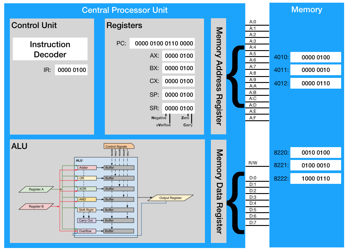
Computers are amazing devices and play a significant role in nearly everything that we do. While seemingly complex, the basic architecture of a computer is straight-forward. In this experience, we'll take a look at memory, the central processing unit, the arithmetic logic unit, data and address buses, and examine how a computer processes instructions.
Memory[edit]


Bit Width[edit]
Computer memory, sometimes referred to as primary storage, is divided into units called words. Each word consists of multiple bits (binary digits). Each bit is preserved through the use of a Flip Flop, such as the D-type Flip Flop described in W1018 SR Latch. The bits are ordered into a fixed-size piece of data (a word) and accessed as a single unit. In the image each word consists of eight bits, and we refer to this as the bit-width of the machine. (For example, many of you may have "64-bit machines", the 64 bits refers to the bit-width of the words in memory and the ability of the processor to handle each word as a single unit.)
Addressable Memory[edit]
Accessing memory requires that each and every word has a unique address, which we call the memory address. Addresses are generally linear, beginning at zero, and increase for each available word in memory. In the image the address is shown on the left-hand side as "4010".
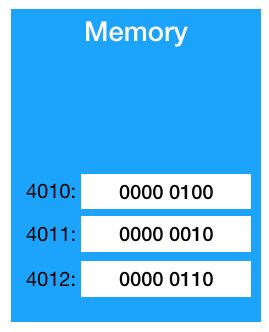
The image on the left shows how addresses increase sequentially. Three words are shown, with addresses (in hexadecimal) of 4010, 4011, and 4012.
The Address Bus[edit]
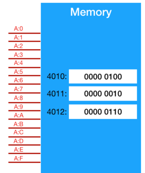
The CPU accesses one word of memory at any given time. In order to specify which of the many words should be accessed, the address is specified on the address bus. The bus specifies, in binary, the address in which we are interested. Each "wire" is either high or low. In combination, the high/low values on the bus indicate the address. As usual, the least significant bit is labeled as 0 (A:0).
The Data Bus[edit]
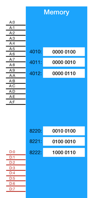
While the address bus specified the address in which we are interested, it is the data bus which actually moves the data from/to primary storage. Note that in the case of our example, there are sixteen bits required on the address bus to specify the word in which we are interested, because this computer can access words. The data bus, however, is only eight bits wide, because each word contains exactly eight bits.

The Read/Write Flag[edit]
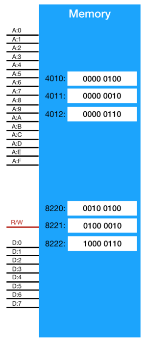
The data bus can either transfer data to main memory or from main memory, but not both at the same time. In order to specify the direction, we use a read/write flag. (A flag is a term that generally represents exactly one of two possible states.)
The Arithmetic Logic Unit[edit]
The Arithmetic Logic Unit, often abbreviated as ALU, is responsible for accepting one or two operands, performing either an arithmetic or logical operation, and then providing the result. These calculations are performed using the logic gates which we've previously studied, such as AND, OR, NOT, XOR, and binary addition.

A register is a quickly accessible location which can be directly accessed in a process which is much faster than accessing main memory. In the case of the ALU, there are two input registers and one output register. In order to perform an operation the input operands are sent to the input registers (Register A and Register B), and, after a brief propagation delay, the output is made available in the Output Register.
The Central Processing Unit[edit]

The Central Processing Unit, often abbreviated as CPU, is responsible for executing the instructions of a program, including those of the operating system. The CPU contains several internal registers. Some of these registers are general purpose and may be used for temporarily holding operands. In our example CPU, the general purpose registers are labeled as AX, BX, and CX. Other registers have a special, dedicated purpose. In our example CPU, these are:
- The instruction register: It is responsible for processing an instruction from memory by understanding what steps are required to realize the specified operation.
- The program counter or PC: It is responsible for pointing to the next instruction to be fetched from main memory. As such, the width of this register will be the same as the width of the address bus.
- The stack pointer: It is responsible for pointing to the next free position on the stack (a data structure that we'll cover in a later experience).
- The status register: It contains the status of a recent operation, such as whether or not the result is zero, negative, or if there was an overflow condition.

For further information regarding the status register see Jump Instructions.
The Instruction Cycle[edit]
Digital computers generally follow a standard cycle, called the Fetch-Decode-Execute cycle. It is the basic operational process of a computer. From boot-up until shut down, the CPU (central processing unit) will retrieve a program instruction from memory, determine what the instruction means and how to fulfill that instruction, and then execute the necessary steps before repeating the cycle.
Fetch[edit]
The next instruction is fetched from the memory address that is currently stored in the program counter (PC). The instruction is stored in the instruction register (IR). The PC is then incremented.
Decode[edit]
The instruction is decoded by the instruction decoder. If additional memory accesses are required to read operands, it happens here.
Execute[edit]
The instruction is executed by the control unit which sends a sequence of signals to the relevant function units of the CPU such as reading values from registers, passing them to the ALU to perform mathematical or logical functions, and writing the results back to a register. The control unit may accept input from the ALU and update the program counter to a different address if so indicated before continuing to the next cycle.
An Example[edit]
Let's consider an example of what occurs inside the computer when we execute the following:
Let's assume that the variable is stored in location 0x4010, is stored in location 0x4011, and is stored in location 0x4012. This single statement is essentially instructing the computer to:


- Access the variable
- Access the variable
- Add the values of and
- Store the sum in the variable

Within the computer, this may appear as:
LDAX [4010]
LDBX [4011]
ADDBX
STAX [4012]
The actions carried out by the CPU will be as follows:
- Load the AX register with the value stored in main memory at address 0x4010
- Fetch
- The address in the Program Counter (PC) is placed on the memory address bus
- The address is carried across the address bus to main memory
- Set the memory read/write flag to read
- The instruction located at the specified address is placed on the memory data bus
- The instruction is carried across the data bus to the memory data register
- The CPU transfers the instruction from the memory data register to the Instruction Register (IR)
- The address in the PC is incremented
- Decode
- The CPU decodes the instruction in the instruction register
- The CPU executes a plan to fulfill the instruction
- Execute
- Place the address 0x4010 in the memory address register
- The address is carried across the address bus to main memory
- Set the memory read/write flag to read
- The data located at the address 0x4010 are placed on the memory data bus
- The data are carried across the data bus to the memory data register
- The CPU transfers the data from the memory data register to the AX register
- Fetch
- Load the BX register with the value stored in main memory at address 0x4011
- Fetch
- The address in the Program Counter (PC) is placed on the memory address bus
- The address is carried across the address bus to main memory
- Set the memory read/write flag to read
- The instruction located at the specified address is placed on the memory data bus
- The instruction is carried across the data bus to the memory data register
- The CPU transfers the instruction from the memory data register to the Instruction Register (IR)
- The address in the PC is incremented
- Decode
- The CPU decodes the instruction in the instruction register
- The CPU executes a plan to fulfill the instruction
- Execute
- Place the address 0x4011 in the memory address register
- The address is carried across the address bus to main memory
- Set the memory read/write flag to read
- The data located at the address 0x4011 are placed on the memory data bus
- The data are carried across the data bus to the memory data register
- The CPU transfers the data from the memory data register to the BX register
- Fetch
- Add the current contents of AX to BX, and place the sum in AX
- Fetch
- The address in the Program Counter (PC) is placed on the memory address bus
- The address is carried across the address bus to main memory
- Set the memory read/write flag to read
- The instruction located at the specified address is placed on the memory data bus
- The instruction is carried across the data bus to the memory data register
- The CPU transfers the instruction from the memory data register to the Instruction Register (IR)
- The address in the PC is incremented
- Decode
- The CPU decodes the instruction in the instruction register
- The CPU executes a plan to fulfill the instruction
- Execute
- The CPU transfers the data from the AX register to the ALU's Register A
- The CPU transfers the data from the BX register to the ALU's Register B
- The CPU uses a combination of control signals to specify that it's interested in the add function
- The ALU places the sum of Register A and Register B into its Output Register
- The CPU transfers the contents of the ALU's Output Register to the AX register
- Fetch
- Store the contents of register AX into main memory at address 0x4012
- Fetch
- The address in the Program Counter (PC) is placed on the memory address bus
- The address is carried across the address bus to main memory
- Set the memory read/write flag to read
- The instruction located at the specified address is placed on the memory data bus
- The instruction is carried across the data bus to the memory data register
- The CPU transfers the instruction from the memory data register to the Instruction Register (IR)
- The address in the PC is incremented
- Decode
- The CPU decodes the instruction in the instruction register
- The CPU executes a plan to fulfill the instruction
- Execute
- Place the address 0x4012 in the memory address register
- The address is carried across the address bus to main memory
- Place the contents of the AX register into the memory data register
- The data are carries across the data bus to main memory
- Set the memory read/write flag to write
- The contents of memory data register are written (stored) in main memory at address 0x4012
- Fetch
Key Concepts[edit]

- Main memory in a computer is sometimes referred to as primary storage
- Main memory is divided into fixed-size pieces of data called words
- Each word consists of multiple bits (binary digits)
- The number of bits in a word is referred to as bit-width
- Each bit may be represented by a single D-type Flip Flop
- Accessing memory requires that every word has a unique address; we call this the memory address
- The address bus transfers the requested address from the CPU to main memory
- The data bus transfers data to/from main memory
- The read/write flag specifies whether we want to read from memory or write to memory
- The Arithmetic Logic Unit (often abbreviated ALU) performs a calculation on one or two operands
- The calculations are performed using logic gates such as AND, OR, NOT, XOR, and binary addition
- A register is a quickly accessible location which can be directly accessed in a process which is much faster than accessing main memory
- The ALU receives input from a local Register A and Register B. When the ALU completes its calculation, it places the result in its Output Register.
- The Central Processing Unit, often abbreviated as CPU, is responsible for executing the instructions of a program
- The CPU contains several internal registers:
- The Instruction Register, often abbreviates as IR, is responsible for processing an instruction from memory and assists in decoding the instruction
- The Program Counter, often abbreviated as PC, is responsible for pointing to the next instruction to be fetched from memory
- The Stack Pointer points to the next free position on the stack
- The Status Register contains the status of a recent operation, such as whether or not the result is zero, negative, or whether there was an overflow condition
- The instruction cycle consists of three steps:
- Fetch: The next instruction is fetched from the memory address currently stored in the PC and placed in the IR. The PC is then incremented.
- Decode: The instruction is decoded. If additional memory accesses are required to read operands, it happens here.
- Execute: The instruction is executed by the control unit making use of the ALU as required. The PC may also be updated if so indicated.
Exercises[edit]
- M1022-10 Complete Merlin Mission Manager Mission M1022-10.